Co overview
CPU设计结构概览
---
Hardware of Computer Organization
---
flowchart TB
subgraph LG[逻辑门]
direction LR
Boo(Boolean Logic)
subgraph Tran[Transistor]
direction LR
Ele(Electrodes - output)
Cont(Control wire - input)
click Ele href "#transistor" "跳转"
click Cont href "#transistor" "跳转"
end
Boo & Tran -->|consist|Gate
NOT(NOT)
AND(AND)
OR(OR)
XOR(XOR)
Gate(Logic Gate)
Gate --o|contains|NOT & AND & OR & XOR
click NOT href "#not-gate" "跳转"
click AND href "#and-gate" "跳转"
click OR href "#or-gate" "跳转"
click XOR href "#xor-gate" "跳转"
click Gate href "#logic-gate" "跳转"
end
subgraph Binary[二进制]
direction LR
Bi(binary) --o|represents|Float(float) & Num(num) & ASCII(characters<br> ASCII) & Unic(all languages<br> 16-bit Unicode) & BiOthers(symbols, sounds<br> colors, graphics etc.)
click Bi href "#binary" "跳转"
click float href "#float" "跳转"
click ASCII href "#ascii" "跳转"
end
subgraph ALU[算数逻辑单元]
direction TB
subgraph AU[Arithmetic Unit]
HAdder(Half Adder)
FAdder(Full Adder)
aluOthers(Others:<br>减法, 错位减法<br>负, 增量+1<br>减量-1, 无改变)
click HAdder href "#half-adder" "跳转"
click FAdder href "#full-adder" "跳转"
click AU href "#arithmetic-unit" "跳转"
end
subgraph LU[Logic Unit]
LUZero(Zero)
Overf(Overflow)
Negative(Negative)
click LUZero href "#logic-unit" "跳转"
end
ALUInputA[Input A<br>8 bits]
ALUInputB[Input B<br>8 bits]
subgraph ALUOperation[Operations]
direction TB
ALUOPCode(Operation Code<br>4 bits)
ALUInstructions(Instructions)
ALUOPCode -->|correspond|ALUInstructions
click ALUOPCode href "#alu-operation-code" "跳转"
end
subgraph ALUOutput[Output]
ALUOutputValue[Output Value<br>8 bits]
ALUFlags(Flags<br>1 bits)
end
AU --o ALUOPCode
LU --o ALUFlags
ALUInputA & ALUInputB --> ALUOperation ---> ALUOutput
click ALUFlags href "#alu-flags" "跳转"
end
subgraph Memory[Memomy]
direction TB
subgraph Latch
direction LR
LatchNode(Latch)
subgraph LatchAttr[Latch Attr]
direction TB
LatSet(set)
LatReset(reset)
LatSet ~~~ LatReset
end
LatchNode --o|wire|LatchAttr
end
subgraph GatedLatch
direction LR
GLatchNode(Latch Node)
subgraph GLatchAttr[GLatch Attr]
direction TB
GLInput(input)
GLWriteEnable(write enable)
GLInput ~~~ GLWriteEnable
end
GLatchNode --o|wire|GLatchAttr
end
subgraph Register
direction LR
RegisterNode(register)
subgraph RegAttr
direction TB
RegInput(data-input)
RegRead(read)
RegWrite(write)
end
end
subgraph Reg256[256-bit memory]
direction LR
Reg256Node(256-bit Register) --o Multiplexer[multiplexer]
end
click Multiplexer href "#multiplexer" "跳转"
click Reg256Node href "#256-bit-register" "跳转"
Register --o|in a grid|Reg256
Register --o|in a row|Reg8(8-bit Register)
Latch --->|improve|GatedLatch ----|arrange<br>side-by-sidy|Register
RegisterNode --o|wire|RegAttr
RegInput ~~~ RegRead ~~~ RegWrite
Reg256 --->|8 in a row|RAM256(RAM of 256<br>8-bit address)
click RegisterNode href "#register" "跳转"
click LatchNode href "#latch" "跳转"
click GLatchNode href "#gated-latch" "跳转"
click Reg8 href "#8-bit-register" "跳转"
click RAM256 href "#ram" "跳转"
end
Binary ---->|method|ALU
LG ---->|build|ALU
LG ---->|build|Memory
subgraph CPU[CPU]
direction TB
CPUUnit((CPU))
AdCPU((Advanced CPU))
CPUUnit --- AdCPU
subgraph Phases
direction TB
Fetch[①Fetch]
Decode[②Decode]
Execute[③Execute]
Fetch --> Decode --> Execute
Execute -->|Cycle|Fetch
end
Phases -.-|1 Clock/Each Step|Clock[Clock<br>Link and Send Signals to CU<br>keep things in lock-step]
click Clock href "#clock" "跳转"
click AdCPU href "#advanced-cpu-designs" "跳转"
subgraph CPUFlow[flow]
direction LR
IAReg(Instruction Address Register)
InsTable(Instruction Table)
CU(Control Unit)
subgraph IReg[Instruction Register]
direction TB
OptCode(Operation Code)
OptAddr(Operating Addr<br>memory or registers)
end
cpuALU(ALU)
Registers(Registers)
OptCode -.-|②Decode: Operation Code Ref|InsTable
CU --o|③Execute: Enable wire|Registers
cpuALU -->|③Execute: Output<br>Flags:O Z N|CU
CU -->|③Execute: inputA & inputB<br> Operation Code|cpuALU
CU -->|Complete<br>Increment Address by 1|IAReg
click IAReg href "#instruction-address-register" "跳转"
click InsTable href "#instruction-table" "跳转"
click CU href "#control-unit" "跳转"
click OptCode href "#instruction" "跳转"
click Registers href "#cpu-registers" "跳转"
end
click CPUUnit href "#cpu" "跳转"
end
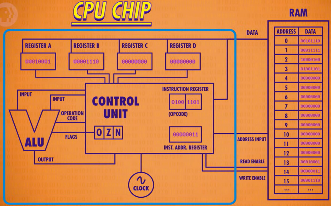
IAReg --->|①Fetch: Input Address<br>寻址|RAM
RAM --->|①Fetch: Output Data<br>写入|IReg
RAM -->|③Execute:Data Wire|Registers
CU --o|③Execute: Enable wire|RAM
IReg --->|②Decode: Activate <br>the Specify Instruction Circuit|CU
Memory ----> RAM
ALU ----->|build|CPU
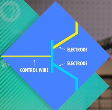
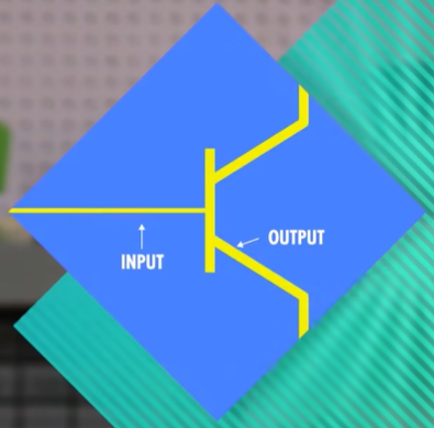
Transistor
Def: Electrically controlled switches.
Picture of Transistor:
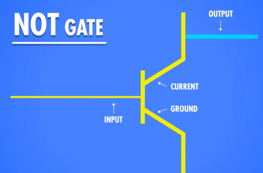
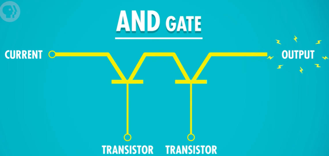
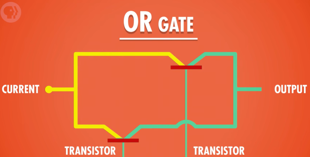
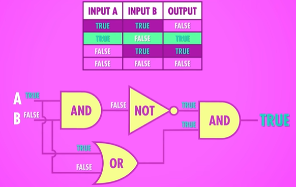
Logic Gate
Def: Operations that implement boolean logic in circuit level.
Not Gate
And Gate
Or Gate
XOR Gate
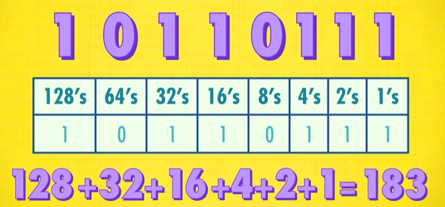
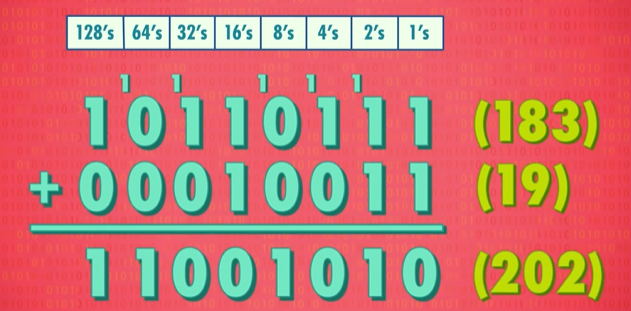
Binary
def: A math method representing more information through two values. Each digit’multiplier is two times larger than the one to the right.
example:
addtion rule:
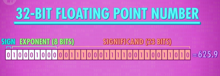
Float
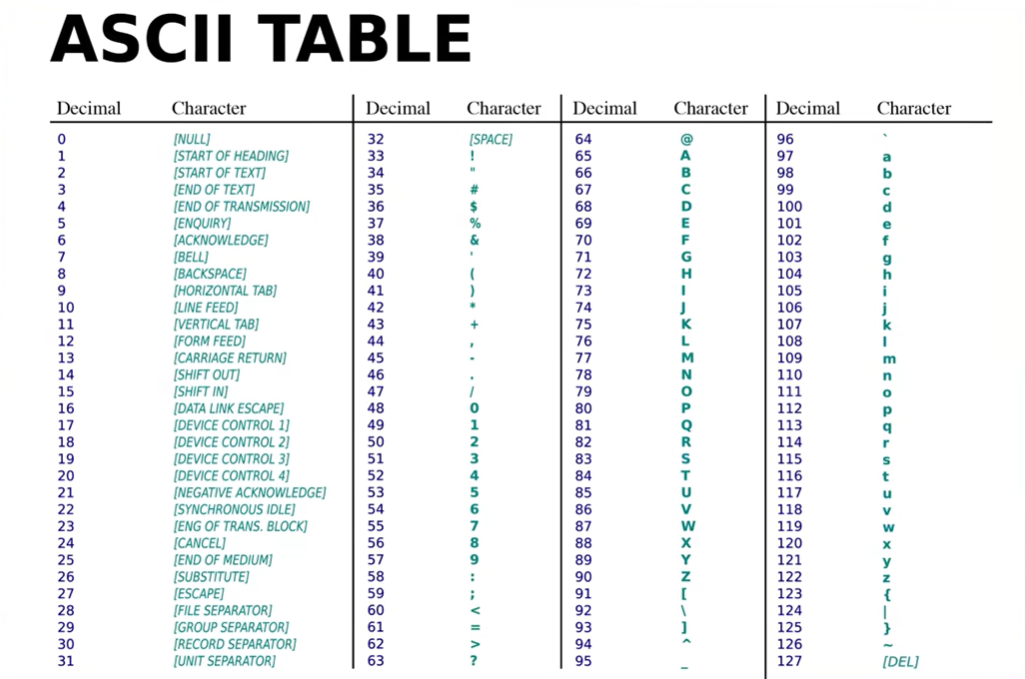
ASCII
def: 7-bit code. contains: punctuation, digits, letters.
limit: Only designed for english.
ALU
def: A unit for computation, consisting of two unit - an arithmetic unit and a logic unit.
Arithmetic Unit
def: Handling all numerical operations in a computer, like addition, subtraction and increment operation.
Processing data bit by bit.
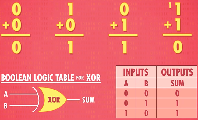
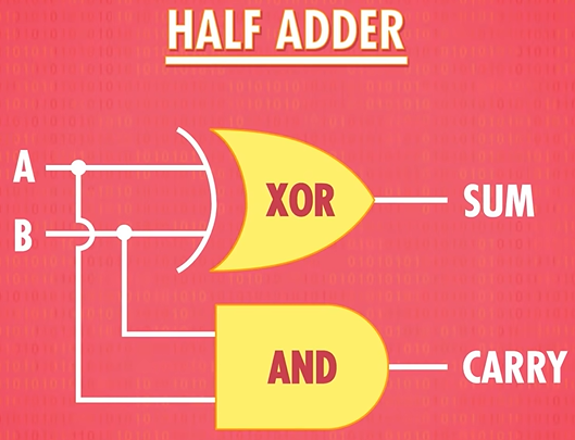
Half Adder
Two input and two output.

The course of build a half adder.
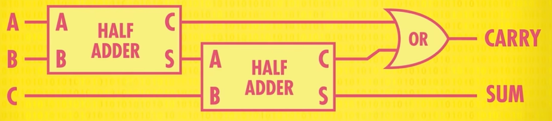
Full Adder
Three input and two output. Able to manage the addition of next column.
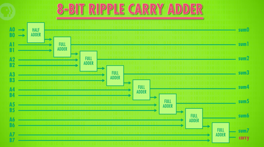
8-Bit Ripple Carry Adder
built by half adder and full adder
Logic Unit
It performs simple numerical tests, like checking if a number satisfies certain condition.
Example:
zero: check if the number is zero. 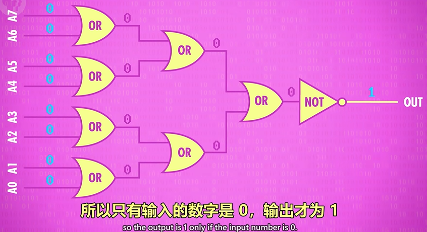
ALU Operation Code
def: In this case, it uses 4 bits.
For example 1000 might be the command to add, while 1100 is the command for subtract.
ALU Flags
def: 1-bit outputs for particular states and statuses.
For example, 1 - 1 = 0 sets the Zero Flag to True(1).
Memory
def: The part of a computer in which information or programs are stored either permanently or temporarily, or the amount of space available on it for storing information. Type1. RAM: Random Access Memory. Which stores things like game state - as long as the power stays on.
Type2. Persistent Memory: It can survive without power.
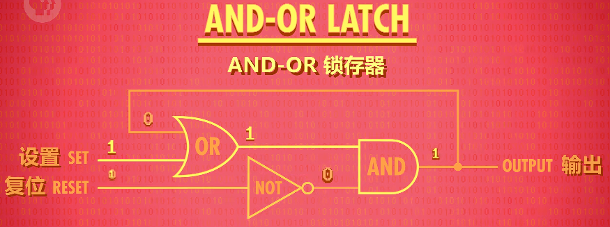
Latch
def: built by logic gate and used to store one bit of information.
This is called a “latch” because it “latches onto” a particular value and stays that way. The action of putting data into memory is called writing, whereas getting the data out is called reading.
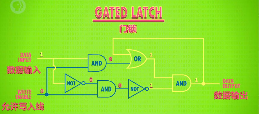
Gated Latch
Register
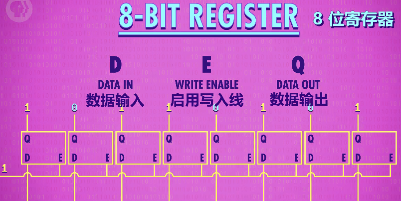
def: A group a latches operating side-by-side is called a register, which holds a single number, and the number of bits in a register is called its width.
functions required:
- input [data for write]
- read [data stored]
- write [enable write the data in input]
8-bit Register
Arrangement: n-bit put n latches in a row
- data wire - n
- output wire - n
- enable wire - 1
- in total: 2n + 1
| wire | num | mem |
|---|---|---|
| data wire | n | input data |
| output wire | n | read |
| write enable wire | 1 | enable write |
| in total | 2n+1 |
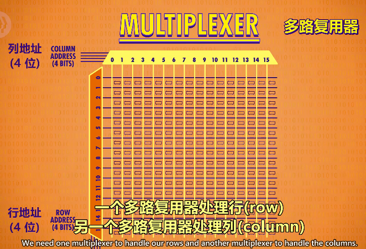
256-bit Register
Arrangement: Use matrix, put latches in an n x m grid.
specify certain latches by row wire and column wire then it comes to the previous pattern.
- row wire - n
- column wire - m
- write enale wire - 1
- read enale wire - 1
- data wire - 1
- in total n+m+3
| wire | num | mem |
|---|---|---|
| row wire | n | |
| column wire | m | |
| write enable wire | 1 | write |
| read enable wire | 1 | output |
| data wire | 1 | input data |
| in total | n+m+3 |
16x16 Latch Matrix
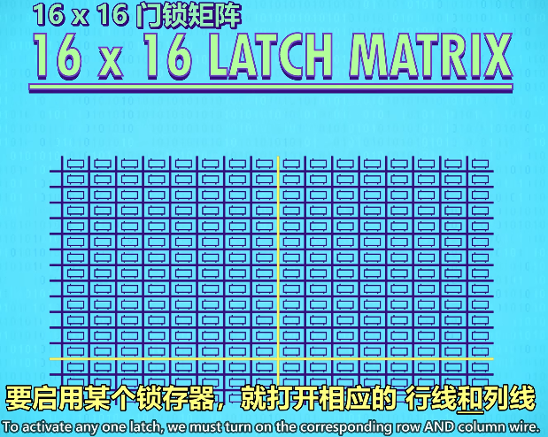
Picture of the latch at the intersection of the two active wires
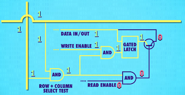
Multiplexer
Multiplexer(多路复用器): convert from an address into something that selects the right row or column.
Things like 1000 0010, means row 8 and column 2.
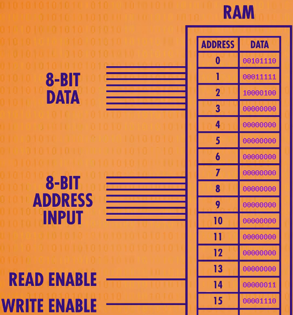
RAM
An important property: We can access any memory location, at any time, and in a random order.
For this, it’s called Random-Access Memory or RAM.
Picture of 256-bit of Memory
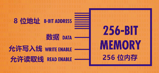
Put 8 256-bit Memory in a row so that store an 8-bit number as a byte.
When it comes to store address, each memory stores one bit on the same address, there’s 8 memory to store so it is an 8-bit number.
This is a SRAM(Static Random-Access Memory) which uses latches.
Other types of RAM, such as DRAM, Flash memory, and NVRAM. They use different circuits to store the individual bits. For example, using different logic gates, capacitors, charge traps, or memristors.
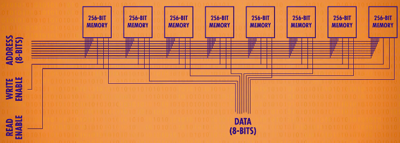
Think of it as a uniform bank of addressable memory. It have 256 addresses, and at each address we can read or write an 8-bit value.
CPU
def: The Central Processing Unit.
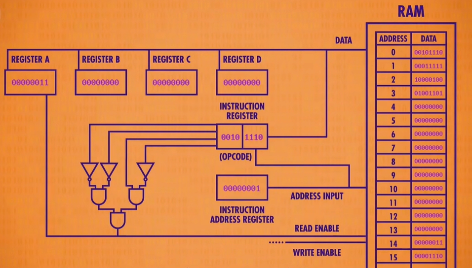
Simplified CPU:
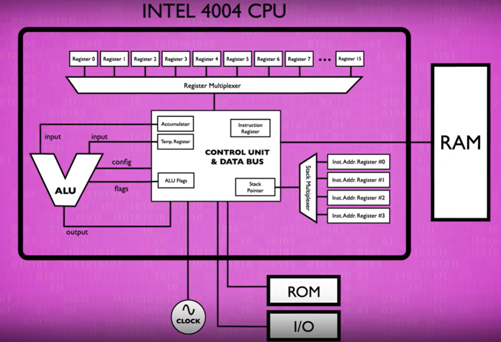
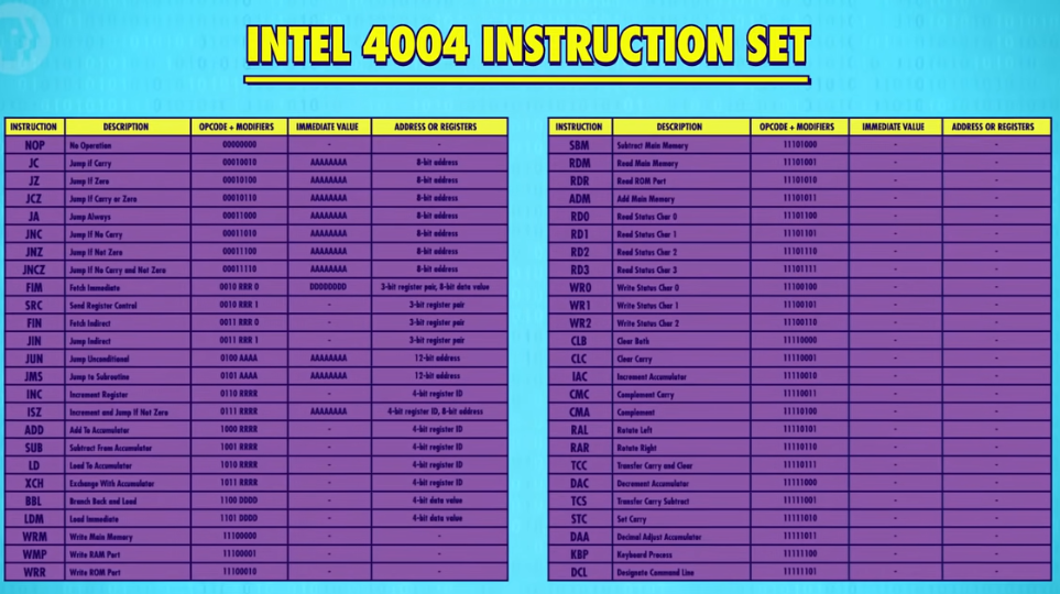
Intel 4004 CPU
CPU-Registers
def: Thery are used to temporarily store and manipulate values.
- When we first boot up our computer, all of registers start at 0.
Instruction Address Register
def: A register to keep track of where we are in a program, stores the memory address of the current instruction.
Instruction Register
def: A register to store the current instruction.
At this hypothetical example, the instruction stored is an 4 bits opcode in register.
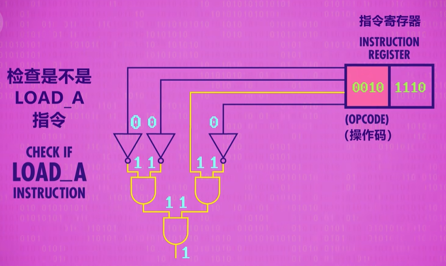
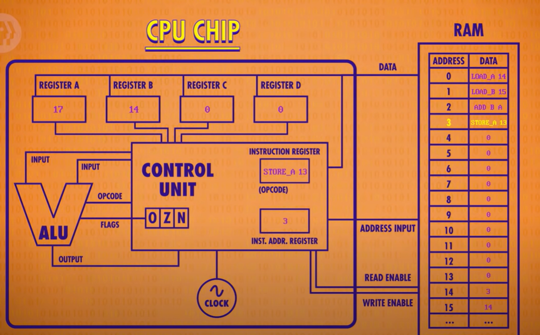
Control Unit
def: Like everything else we’ve built, it too is made out of logic gates.
Different instructions are decoded by different logic circuits, which configure the CPU’s components to perform that action.
Also, the Control Unit has internal registers to temporarily save the output from ALU, in case of the new value would ripple back into the ALU and then keep doing the action to itself. After turning off the ALU, then write the value into the destination register.
Example: Check if Load_A Instruction
Clock
def: Transition the CPU through its fetch, decode and execute phases. Take the responsibility of keeping the CPU ticking along.
The clock triggers an electrical signal at a precise and regular interval. The sinal is used by the Control Unit to advance the internal operation of CPU, keeping everything in lock-step.
The speed at which a CPU can carry out eacho step of fetch-decode-execute cycle is called its Clock Speed. This speed is measured in Hertz - a unit of frequency. One Hertz means one cycle per second.
Overclocking
Modify the clock to speed up the tempo of the CPU. Chip makers often design CPUs with enough tolerance to handle a little bit of overclocking.
Underclocking
Application: Sometimes it’s not necessary to run the processor at full speed. By slowing the CPU down, it can save a lot of power.
Dynamic Frequency scaling
动态调整频率
Processors can increase or decrease their clock speed based on demand.
Instruction
Strategies to have bigger instructions:
- The Instruction Length: with more bits, like 32 or 64 bits.
- Variable Length Instructions
- Execute Immediately: see an instruction that needs no extra values
- Immediate Value: saved immediately behind the instruction that needs value in memory.
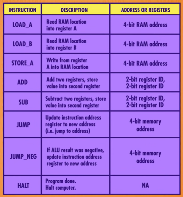
Instruction Table
def: Assign an ID to each instruction supported by CPU. The ID is called “operation code” or opcode for short.
Hypothetical Example:
We use the first four bits to store the “operation code”. And the last 4 bits specify where the data for that operation should come from - this could be register or an address in memory.
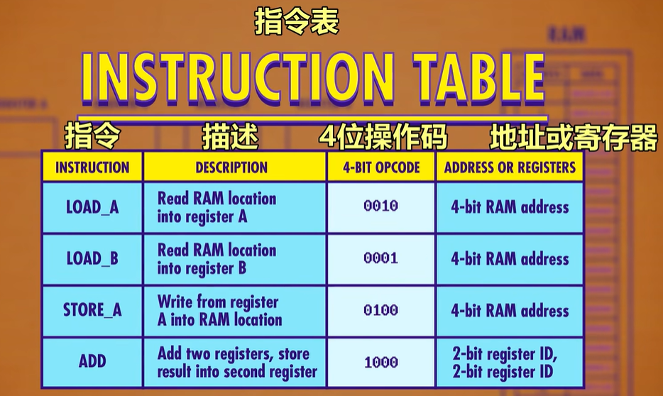
Basic Instruction:
Real Instruction Example:
Instruction Execute View
Origin View:
Easy-Understand View:
Advanced CPU Designs
Boost performance allowing not only simple instructions to run fast, but also performing much more sophisticated operations.
The ways to Advance CPU:
- Improve the speed of switching transistors
- Design specific circuit to complete sophisticated operation, like divide, game and video codec.
- makes the ALU bigger and more complicated to design.
- CacheAdd cache to enhance the speed of data-input or output.
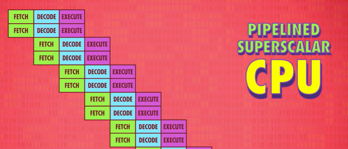
- Instruction Pipelining
- Parallelize
- Out-of-order execution
- Jump instructions
- speculative execution
- branch prediction
- Superscalar Processor
- Execute more than one instruction per clock cycle.
- More ALU
- Multi-core processor
- More CPU
Cache
Scenario: A “load from RAM” instruction might take dozens of clock cycles to complete, and during this time the CPU processor is just sitting there idly waiting for the data. One solution is to put a little piece of RAM right on the CPU – called a cache.
Function: Allows the RAM transmit a whole block of data to CPU and saves it into cache.
- Cache Hit
- Data requested in RAM is already stored in the cache.
- Cache Miss
- Data requested isn’t in the cache, you have to go to RAM.
Dirty Bit
def: A special flag of cache for each block of memory it stores. Record the mismatch between the cache’s copy of the data and the real version stored in RAM, so that everything can get synced up later.
Most often the synchronization happens when the cache is full but a new block of memory is being requested by the processor. 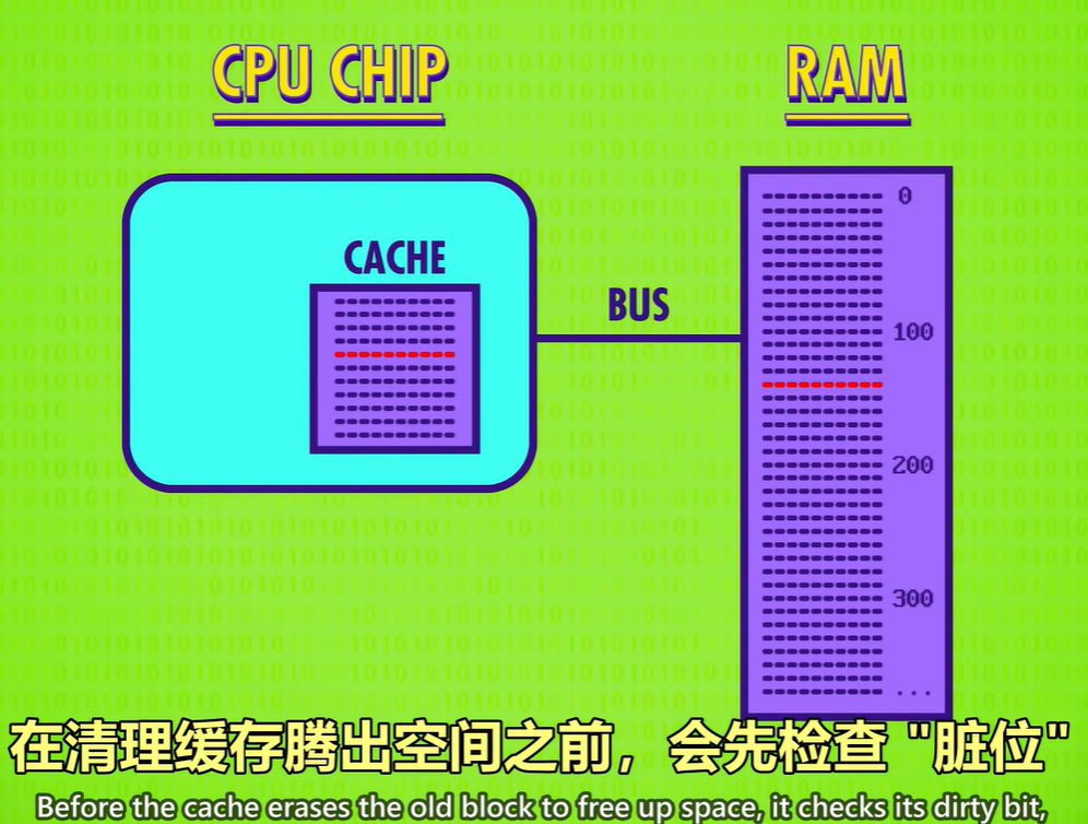
Instruction Pipelining
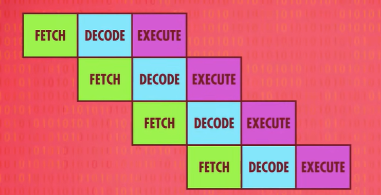
When parallelizing pipelining, this can lead to some tricky problems:
Num.1
- Dependency in the instructions.
- For example, fetch someting that the currently executing instruction is just about to modify.
Solution:
- For example, fetch someting that the currently executing instruction is just about to modify.
- Out-of-order execution
- Dynamically reorder instructions with dependencies, in order to minimize stalls and keep the pipeline moving.
Num.2
- Jump Instructions
- Change the execution flow of a program depending on a value.
- A simple pipelined processor perform a long stall when it sees a jump instruction, waiting for the value to be finalized.
Solutions:
- Speculative execution
- Imagine an upcoming jump instruction as a fork in a road - a branch. Advanced CPUs Guess which way they are going to go and filling their pipeline with instructions based off that guess
- If the CPU guessed wrong, is has to discard all its Speculative results and perform a pipeline flush
- Branch Prediction
- Sophisticated ways to guess which way branches will go, the accuracy of which is often over 90%.
Superscalar Processor
With more ALUs so it can execute many mathematical instructions all in parallel:
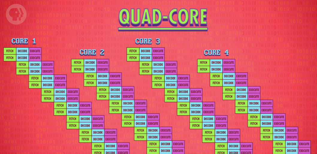
Multi-core Processor
Like dual core or quad core processors. This means there are multiple independent processing units inside of a single CPU chip.
Like having multiple separate CPUs, but for they’re tightly integrated, they can share some resources, like cache, allowing the cores to work together on shared computations.